
Tr3版图三维阅读Layouts in 3D
把平面版图,
立起来读。Read your layout
in three dimensions.
Layout 3D Viewer 把 OA、GDS、OAS 版图变成可以旋转的三维场景。下面用同一个 LC VCO 版图演示:转过来看被遮住的金属,按层拆开看叠层,在一个搜索框里找 pin、子模块和 net。Layout 3D Viewer turns OA, GDS and OAS layouts into a 3D scene you can rotate. One LC VCO layout shows how: turn it to see hidden metal, split it by layer to read the stack, and find pins, submodules and nets from one search box.
为什么做Why
平面版图里,
什么最难看清?What is hardest to see
in a flat layout?
一个 VCO 从多晶硅到顶层厚金属有十几层导体,在二维视图里全部投影到同一个平面上。下面三件事最费时间。A VCO stacks a dozen conductor layers from poly to the thick top metal, and a 2D view projects them all onto one plane. These three things take the most time.
演示片Film
转过来,拆开来,
找到它。Turn it, take it apart,
find it.
中英文版各有配音,随页面语言切换。全片都用同一个 VCO 版图,画面是 Layout 3D Viewer 的实际操作。Separate Chinese and English narration follows the page language. The whole film uses one VCO layout, and every shot is the real Layout 3D Viewer at work.
怎么读How to read
一个版图,
六种读法。One layout,
six ways to read it.
示例是一个 LC VCO:单圈差分电感和放射状地屏蔽,腿间是 4 位开关电容阵列、交叉耦合对和尾管,两侧是去耦电容,外面一圈地环。每个连接点都留了 pin,方便电磁仿真与寄生提取在同一位置对接。The example is an LC VCO: a single-turn differential inductor over a radial ground shield, a 4-bit switched-capacitor array, a cross-coupled pair and a tail between the legs, decoupling caps on both sides and a ground ring around it all. Every connection point carries a pin, so EM and parasitic extraction can meet at the same place.
转过来,拉开层Turn it, then pull the layers apart
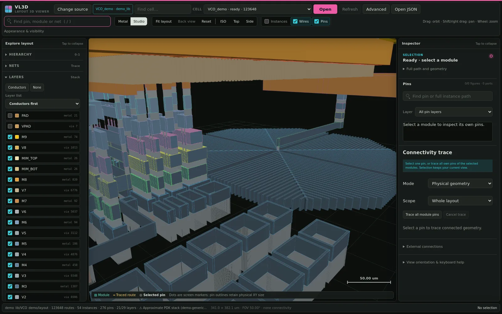
拖动旋转、倾斜,从侧面看到被顶层厚金属挡住的阵列和过孔。拖动时只画顶部几层金属的线框,松手后恢复实体,十几万个图形也能跟手。把层间距拉开,叠层按工艺顺序升起来;拉伸只改显示,XY 尺寸不变。Drag to rotate and tilt, and see the array and vias under the thick top metal from the side. While you drag, only the top metals are drawn as outlines, and solids return when you let go, so a layout of over a hundred thousand shapes still follows the mouse. Stretch the layer spacing and the stack rises in process order; the stretch changes the display only, never XY.
- 拖动时线框Outlines while dragging
- Z 向拉伸Z stretch
按叠层读金属关系Read metal by the stack
层列表从顶层金属排到第一层,每层旁边标着类型和图形数,过孔夹在它连接的两层之间。逐层开关,就能看出一串过孔从哪层起、到哪层止。The layer list runs from the top metal down to metal one, with the type and shape count beside each layer, and every via sits between the two layers it joins. Toggle layers one by one to see where a via stack starts and ends.
- 叠层排序Stack order
- 逐层开关Per-layer toggles
一个搜索框找 pinFind a pin from one box
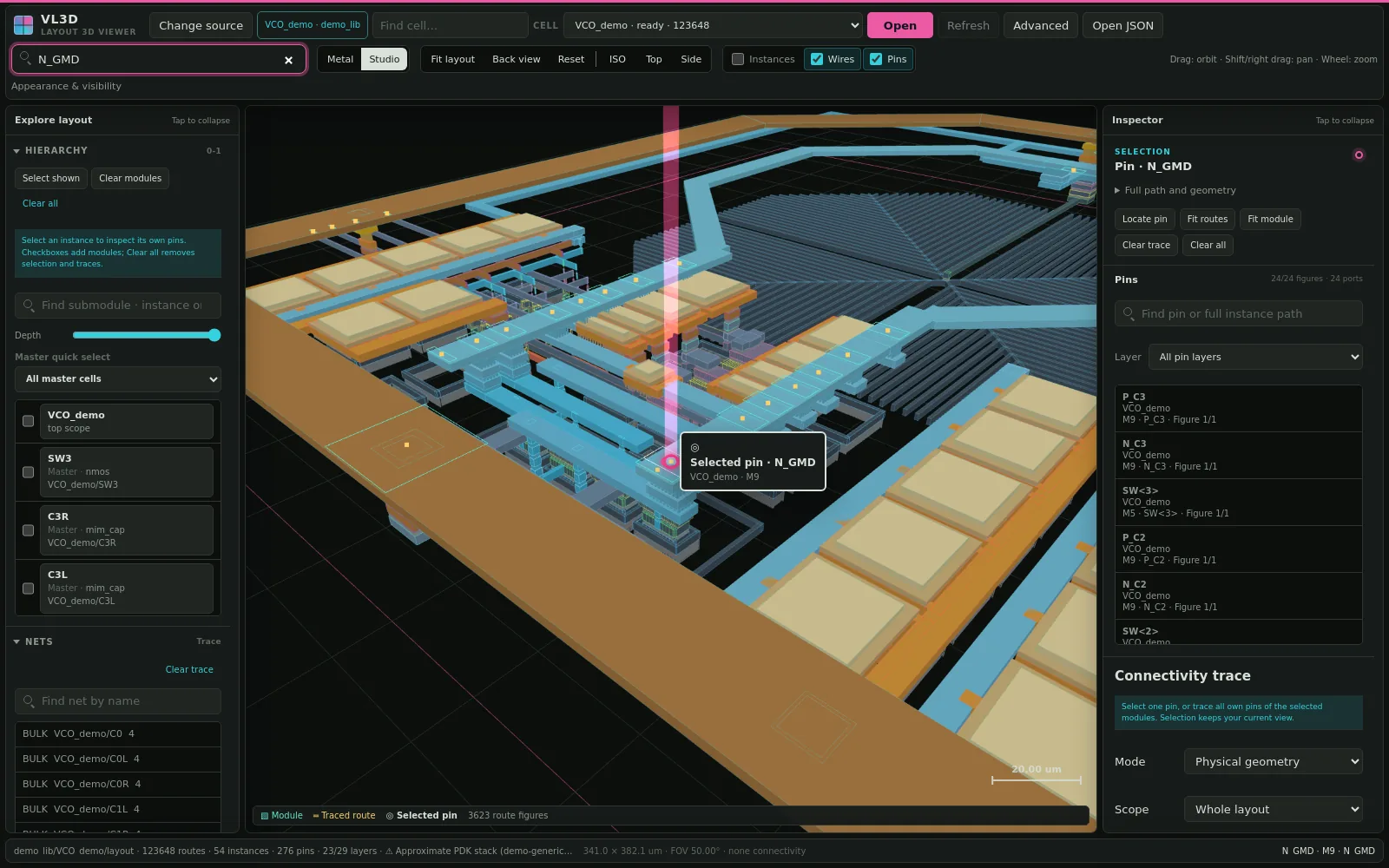
按 / 键进入顶栏搜索框,输入几个字母,pin、子模块和 net 按类别列出。回车后视角平滑飞到目标,pin 上立起一根光柱,屏幕上的光圈闪三下后留下静态环,其余几何淡到背景里。光圈只用 CSS 动画,不额外重绘三维场景。Press / to reach the search box in the toolbar and type a few letters; pins, submodules and nets are listed by kind. Press Enter and the view flies to the match, a light column rises from the pin, an on-screen ring pulses three times and then stays, and everything else fades into the background. The ring is a CSS animation, so the 3D scene is not redrawn for it.
- / 快捷键/ shortcut
- 平滑定位Smooth flight
- 其余淡化Focus fade
找子模块Find a submodule
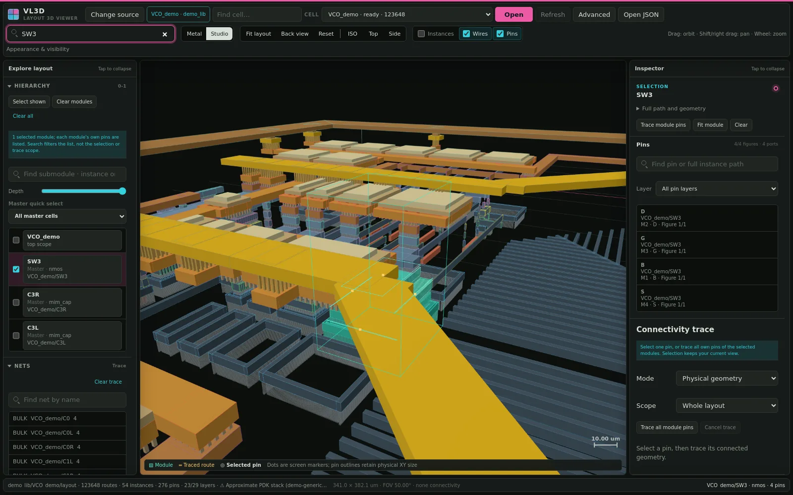
同一个搜索框按实例名、完整路径或 master 名找子模块。选中后画出外框,右侧列出这个模块自己的 pin,可以接着定位或追踪。示例里搜索 SW3,就选中阵列最高位的开关管。The same box finds submodules by instance name, full path or master name. The match gets an outline box and the inspector lists its own pins, ready to locate or trace. In the example, searching SW3 selects the switch of the array's most significant bit.
- 实例 / 路径 / masterInstance / path / master
- 模块外框Module outline
找对应的 netFind the net it belongs to
有电气 net 名的版图,可以直接按 net 名搜索并高亮。没有 net 名时,从 pin 出发按物理几何追踪:相连的电感腿、阵列连线和过孔一起高亮。示例从 N_GMD 追出 3623 个图形;器件边界信息不全的地方,界面标为不完整,不会把不同端子连成一片。If the layout carries electrical net names, search a net by name and highlight it. Without net names, trace from a pin along physical geometry: the connected inductor legs, array straps and vias light up together. In the example, N_GMD traces to 3623 shapes. Where device-boundary data is incomplete, the trace is marked incomplete rather than joining different terminals.
- 按 net 名By net name
- 按物理几何By physical geometry
- Back
换一种外观Switch the look
顶栏的 Metal / Studio 切换渲染风格。Metal 是原来的金属质感;Studio 平涂明亮,顶层金属一种亮色,下层压低饱和度,边线很淡,适合演示和浅色背景。切换只改材质、灯光和配色,不重建几何,不增加渲染开销。过孔默认不画边线,密集版图的锯齿和噪点明显减少。Metal / Studio in the toolbar switches the render style. Metal is the original metallic look; Studio is flat and bright, with one luminous top metal, muted lower layers and faint edges, suited to presentations and light backgrounds. Switching changes materials, lights and colours only, without rebuilding geometry or adding render cost. Vias draw no outlines by default, so dense layouts show far less aliasing and noise.
- Metal
- Studio
- 深色 / 浅色Dark / Light
安装Install
依赖就绪后,
三条命令启动。Once prerequisites are met,
three commands to start.
原生 setup 在用户目录下建隔离的 Python 环境,不升级系统 Python,也不写 OA 或 PDK 目录。发布包自带校验过的 Three.js,生产环境不需要 npm install。Native setup builds an isolated Python environment in the user's data directory. It does not upgrade system Python or write to OA or PDK directories. The release bundles a verified Three.js, so production needs no npm install.
# 检查路径、权限、端口和可选工具# check paths, permissions, ports and optional tools
$ ./bin/vl3d doctor

# 建隔离环境并安装原生依赖# create the isolated environment and install native deps
$ ./bin/vl3d setup --native --install

# 启动原生界面(不需要 Cadence),点 Load example# launch the native interface (no Cadence needed), click Load example
$ ./bin/vl3d gui --no-oa

# 给 agent:机器可读诊断,按第一个 error 处理# for agents: machine-readable report; fix the first error
$ ./bin/vl3d doctor --library /path/to/OA_library --json
- 输入Input
- OA、JSON、GDS、OAS。GDSII 和 OASIS 由 gdstk 导入OA, JSON, GDS, OAS. GDSII and OASIS import through gdstk
- 层映射Layer maps
- 仓库只带通用 profile 和一个虚构示例;真实工艺请提供你自己的 layer profile 或 layer mapOnly a generic profile and a fictional example ship; for a real technology supply your own layer profile or layer map
- 运行环境Runtime
- Node.js 18+,Python 3.6+ 与系统 Tk(缺 Tk 先装,如 CentOS 7 的 python3-tkinter);Linux 原生界面需要 X11/XWayland 和能建立 OpenGL 2.1/GLX context 的驱动或 MesaNode.js 18+, Python 3.6+ with system Tk (install it first if missing, e.g. python3-tkinter on CentOS 7); the Linux native UI needs X11/XWayland and a driver or Mesa that can create an OpenGL 2.1/GLX context
- OA
- 另需可用的 Virtuoso、license、cds.lib 或 lib.defs,以及初始化站点环境的 shell 脚本Also needs a working Virtuoso, license, cds.lib or lib.defs, and the shell script that initializes the site environment
- 离线Offline
- 支持从 wheelhouse 安装,setup 强制 --no-index,不会访问网络Installs from a wheelhouse; setup forces --no-index and never reaches the network
- 诊断Diagnostics
- 错误带 VL3D-E#### 编号,可在排障文档里查原因和建议做法Errors carry VL3D-E#### codes you can look up for cause and fix
- 许可证Licence
- MIT
显示口径About the view
- 示例版图由真实工艺的器件搭成,用于展示阅读方式,未做 DRC 和 LVS 签核。公开画面里的库名、器件名和工艺层名已换成通用名。The example layout is built from real-process devices to show how the viewer reads a layout; it has not been through DRC or LVS sign-off. Library, device and process-layer names on screen are generic.
- 层叠高度与厚度为近似可视化,XY 尺寸与原版图一致。不用于 LVS 签核。Layer heights and thicknesses are approximate; XY dimensions match the original layout. Not for LVS sign-off.
- 连接高亮用于观察几何连接,不表示信号传播仿真。Connection highlights aid geometric inspection; they do not simulate signal propagation.
其他工具Other tools