
Tr6LC VCO 拓扑与电路生成 · v1.1.1LC VCO topologies and circuit generation · v1.1.1
转动旋钮,
看清 2f₀ 对准。Turn the knob.
Align at 2f₀.
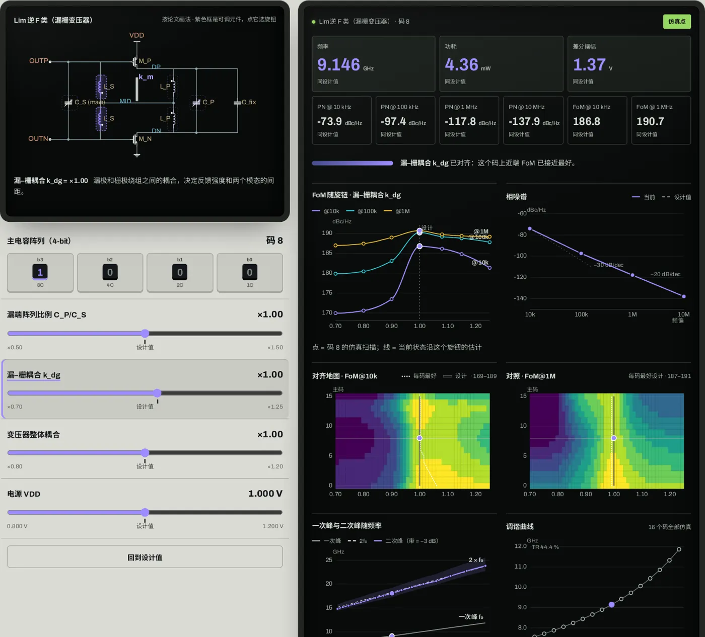
不同结构用不同路径处理二次谐波。Hegazi 与 Murphy 对准共模谐振;Lim 对准漏极差模;Guo 用固定的宽带头部网络;Du 靠两核电感耦合和跨接电容自动跟踪。选结构、转旋钮,观察它们的区别。公开框架提供拓扑、电气图与电路文件生成;本页仪器用于说明机理。Each structure handles the second harmonic differently. Hegazi and Murphy align a CM resonance; Lim aligns a drain differential mode; Guo uses a fixed wideband head network; Du tracks through core-to-core coupling and a cross capacitor. Choose a structure and turn the knob to explore. The public framework provides topologies, electrical graphs and circuit-file generation; this instrument illustrates the mechanisms.
配套页面 · VCO 结构实验室Companion page · VCO Structure Lab
上面是示意,
这里能真的调。Above is an illustration.
Here you tune the real thing.
VCO Design Studio 把五个文献结构变成网表和原理图;VCO 结构实验室把同样五个结构的设计放到网页上,用 400 多次谐波平衡 + 相噪仿真的结果让你直接调参。VCO Design Studio turns five structures from the literature into netlists and schematics. The VCO Structure Lab puts designs of the same five structures on a web page and lets you tune them, backed by more than 400 harmonic-balance and phase-noise simulations.
- 每个结构只给它真实存在的旋钮:4-bit 电容阵列、变压器耦合、2f 返回元件、偏置和电源Each structure gets only the knobs it really has: 4-bit capacitor bank, transformer coupling, the 2f return element, bias and supply
- 对齐地图、一次/二次峰随频率、相噪谱,读数标明是仿真点还是插值Alignment maps, first and second peak vs frequency, phase-noise spectrum; every readout says whether it is simulated or interpolated
- 按论文画的电路图、调参挑战(带答案)、六个设计横向比较和文献索引Schematics drawn after the papers, tuning challenges with answers, a six-design comparison and the literature index
一张电气图One electrical graph
论文里的拓扑,
变成能读的原理图。A paper topology,
as a readable schematic.
五个文献家族、八个变体,另有两个 Class-B 参考。Spectre 网表、原生 OA 构建脚本、界面和 agent 命令行共用一张电气图。装上用户自备的结构包,顶层可照论文排布;没有结构包时自动推导和布局。Five literature families with eight variants, plus two Class-B references. Spectre netlists, native OA build scripts, the interface and agent CLI share one electrical graph. A user-provided structure pack gives a paper-style top level; otherwise it is derived and placed automatically.
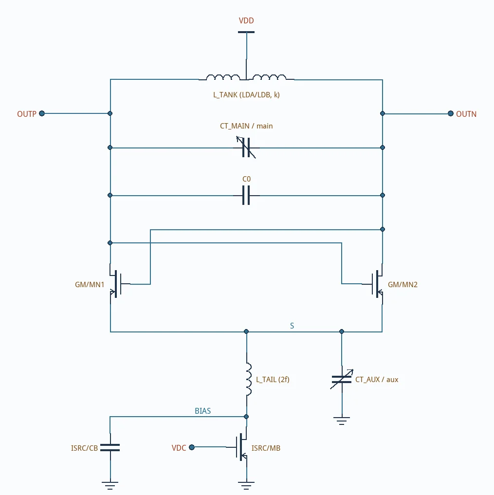
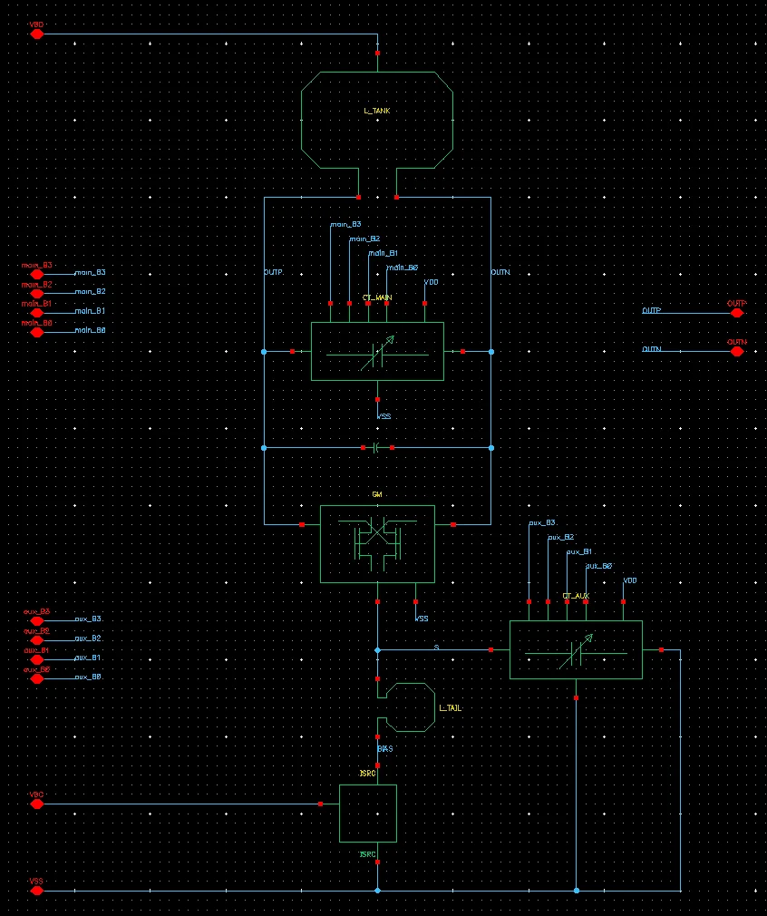
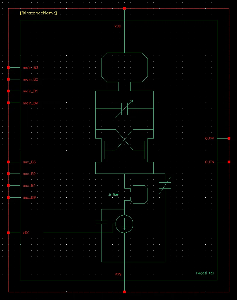
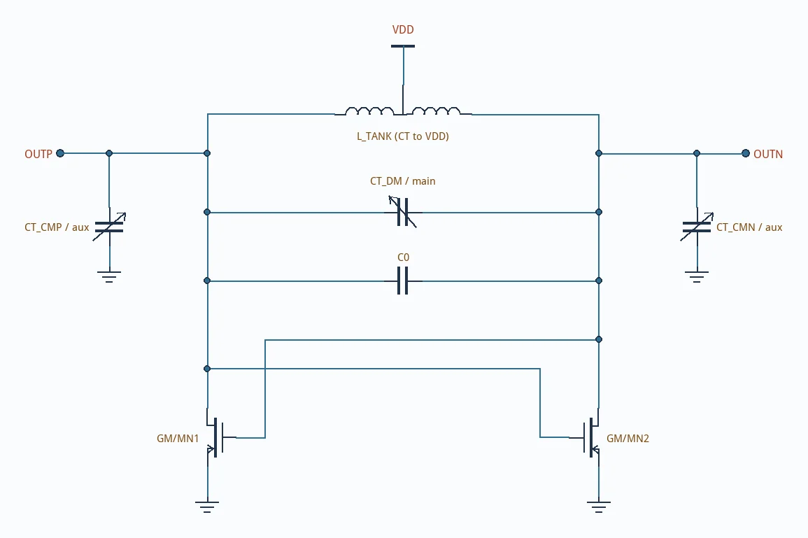
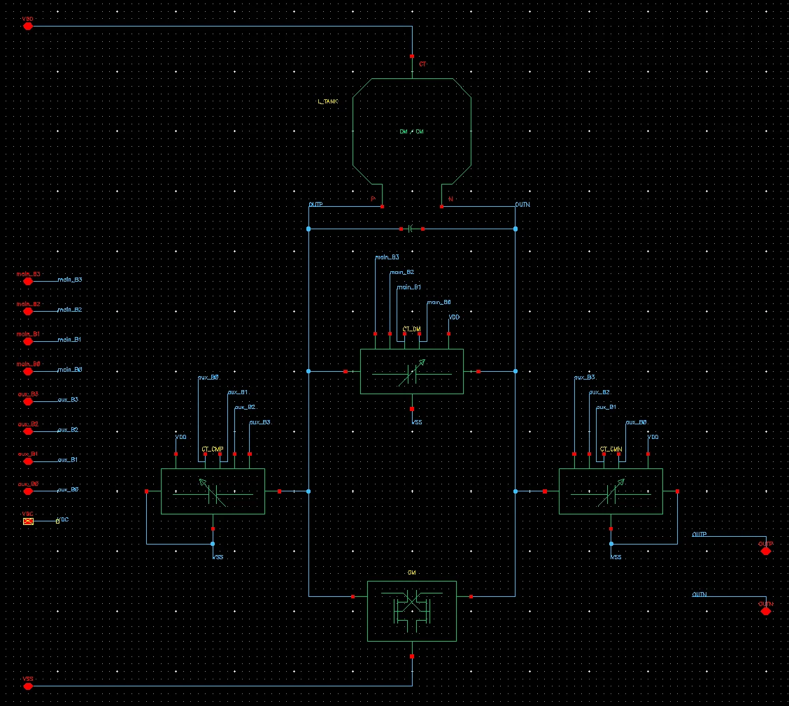
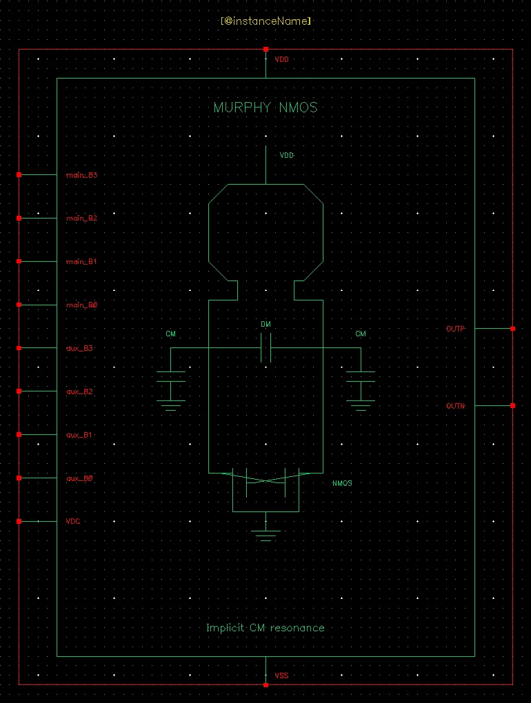
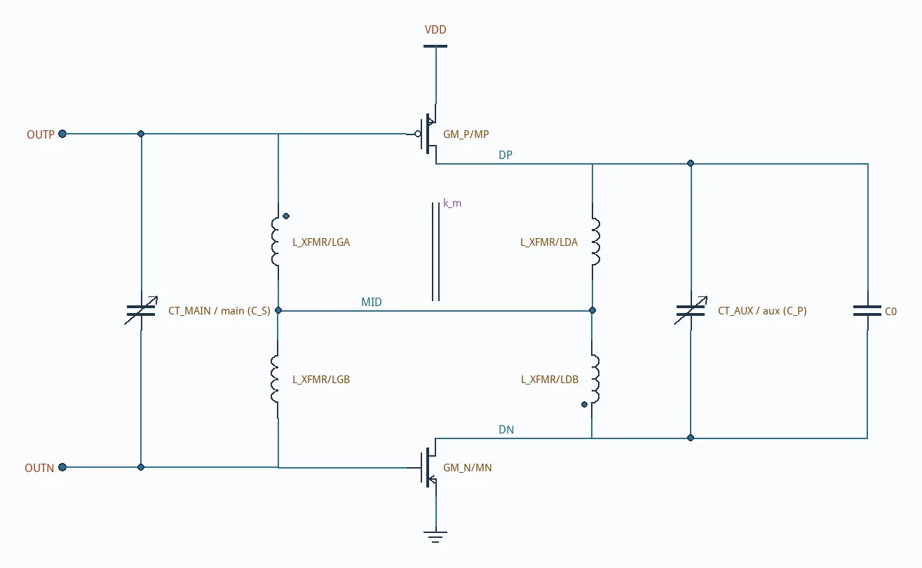
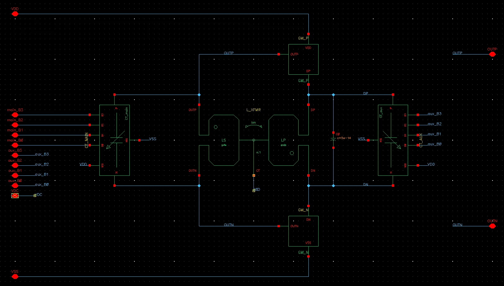
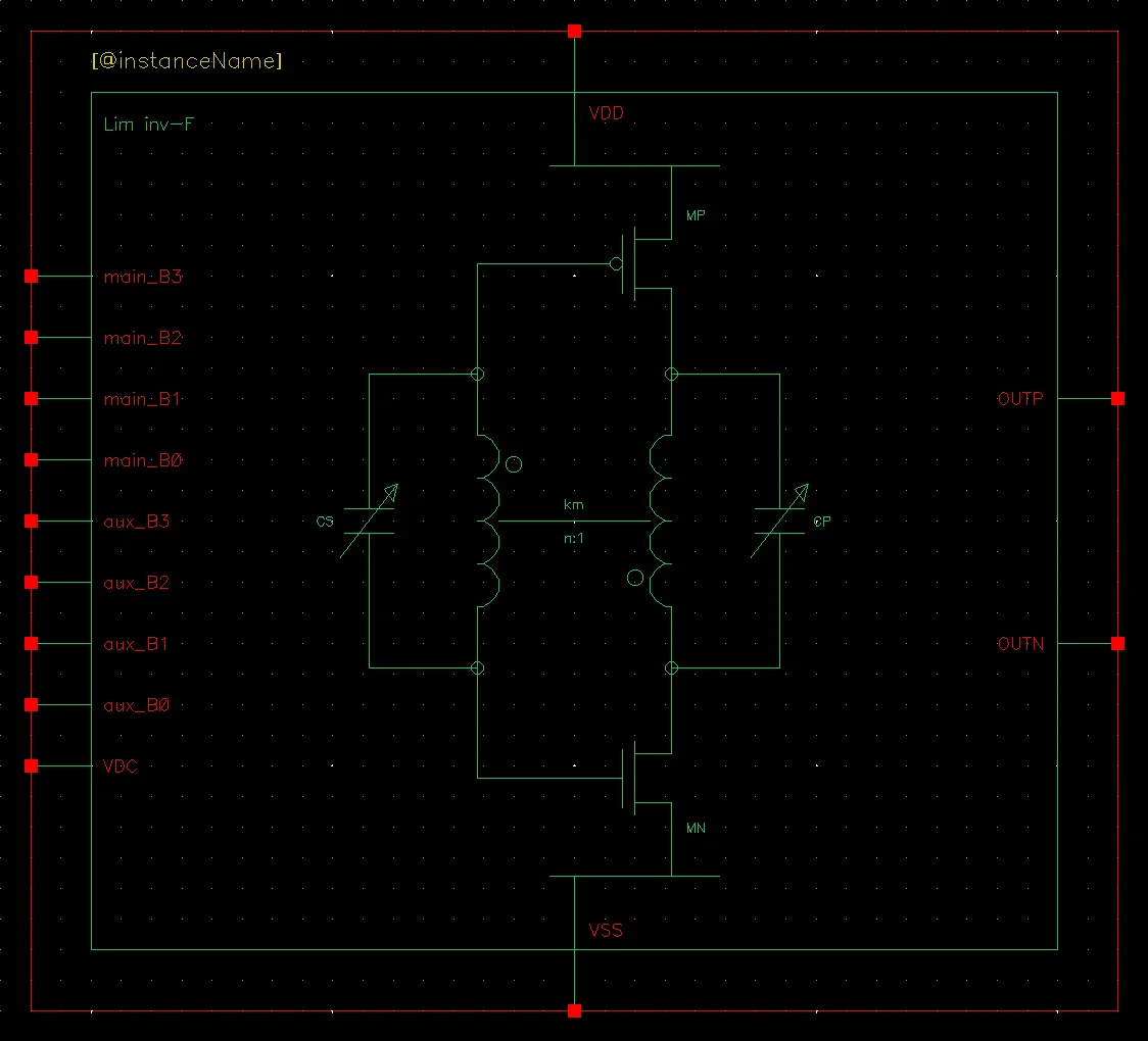
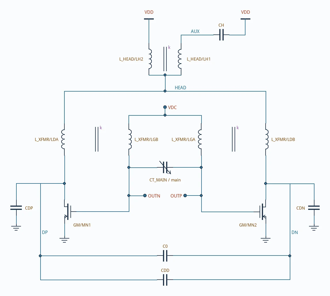
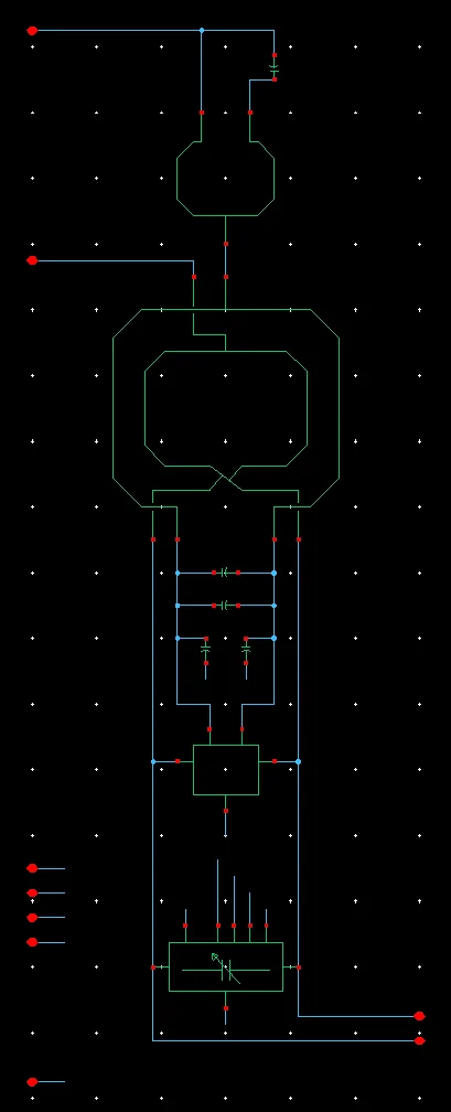
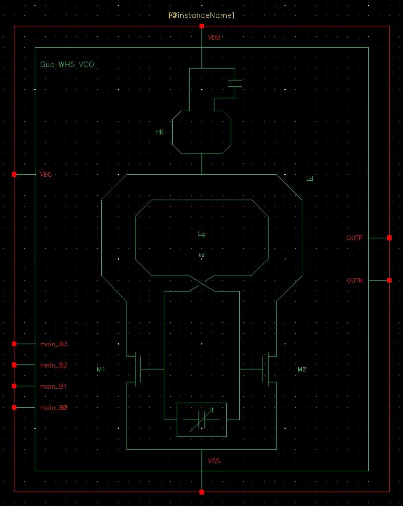
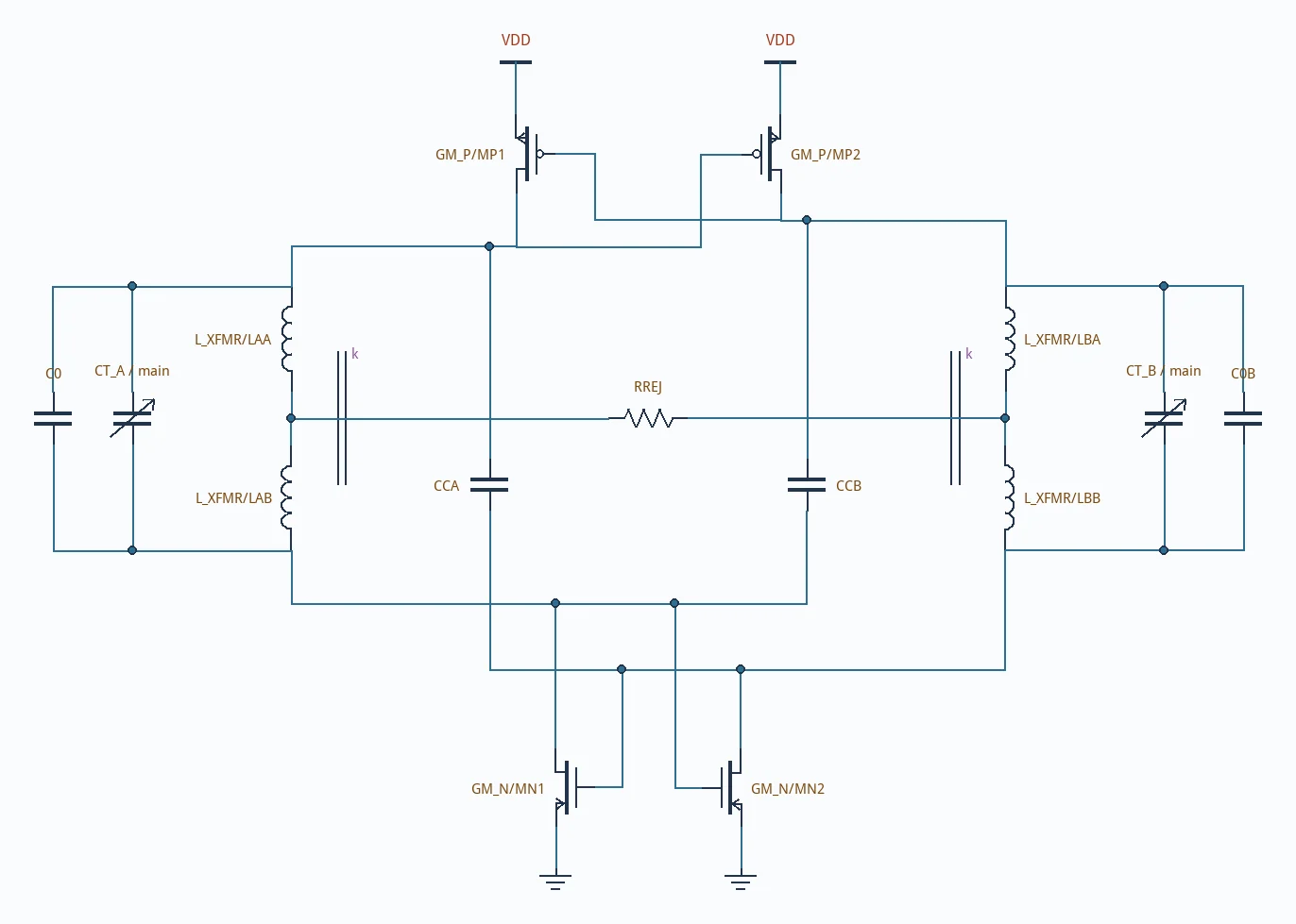
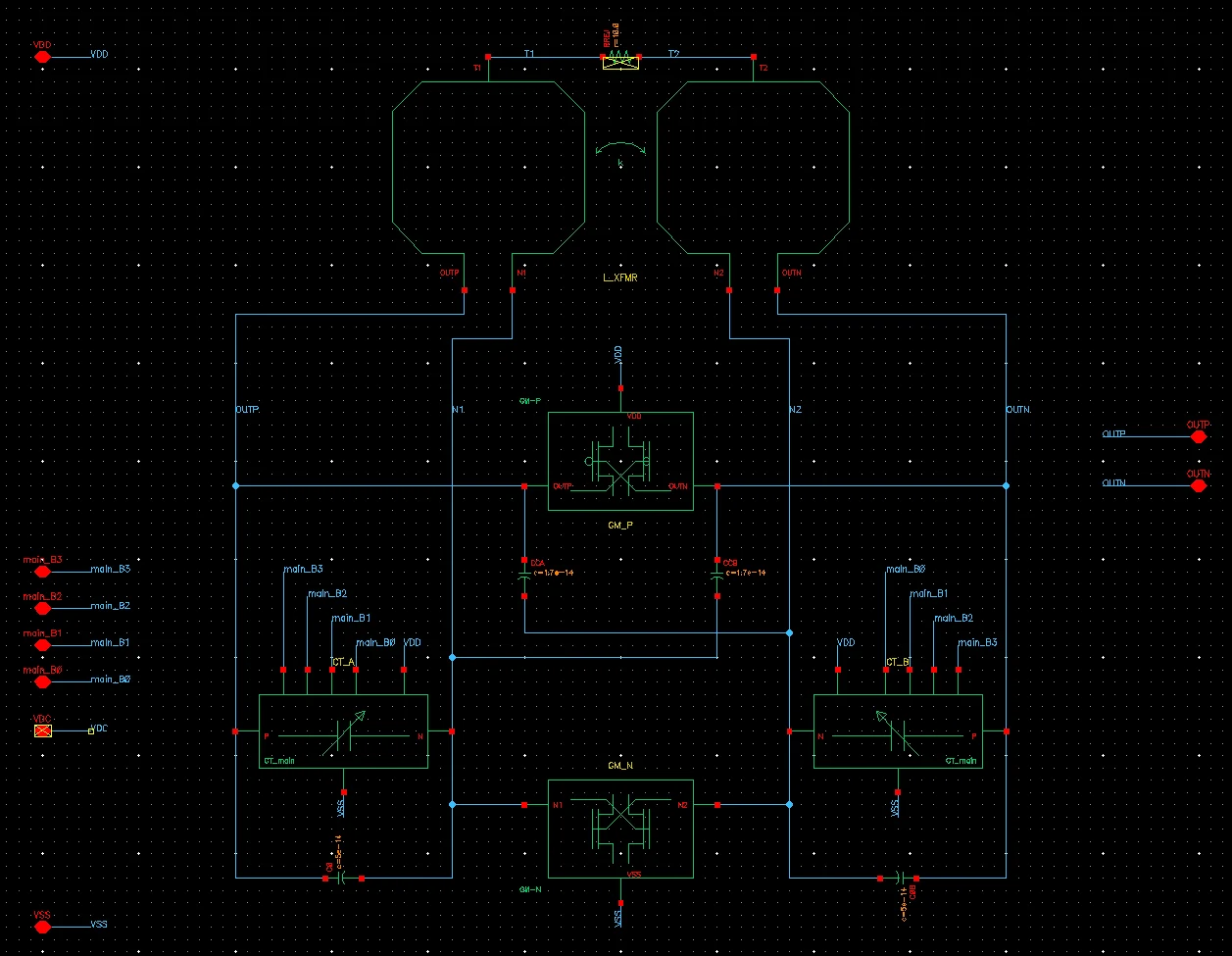
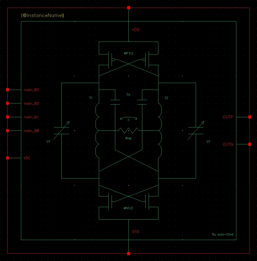
同一个设计的三种视图。原理图和 symbol 是导出到 Virtuoso 的真实截图;论文原图受版权保护,不在此展示,只给出处。Three views of the same design. The schematic and symbol are real Virtuoso screenshots of exported designs; paper figures are under copyright and are cited, not shown.
演示片Film
从二次谐波,
到电气图与原理图。From second harmonics
to graphs and schematics.
中英文版各有配音,随页面语言切换。先看二次谐波对准,再看拓扑、电气图和原生导出流程。Chinese and English versions each have their own narration and follow the page language. See second-harmonic alignment, then topologies, electrical graphs and the native export workflow.
为什么做Why
生成出来的电路,
也得有人能读。A generated circuit
still has to be read.
自动生成一个几百个器件的扁平网表并不难。难的是让工程师打开 Virtuoso 时,看到的东西和论文、和手画的 Class-B 单元一样好读,而且能确认它和仿真用的电路是同一个。Generating a flat netlist of a few hundred devices is easy. The hard part is that an engineer opening Virtuoso sees something as readable as the paper and a hand-drawn Class-B cell set, and can trust it is the same circuit that was simulated.
分层封装Packaged hierarchy
每一级都有
画好的 symbol。Every level has
a drawn symbol.
电感单元里放绕组、显式损耗和全部耦合;绕组用单匝 symbol 表示,管脚和 EM n 端口视图兼容,日后可以直接换成电磁仿真模型。下面四张都是导出后在 Virtuoso 里截的 symbol。Inductor cells hold the windings, explicit loss and every coupling. Windings use a one-turn symbol whose pins stay compatible with an EM n-port view, so an electromagnetic model can be swapped in later. All four below are symbols captured in Virtuoso after export.
验证Verification
先证明等价,
再写 OA。Prove it equal,
then write OA.
把封装好的层次拍平,和电气图逐项比较:器件、层次解析后的等效参数、端子到网络的划分、端口。顶层方案再按原理图编辑器的规则抽取连接:线的 T 形交点才算连接,端子不能落在线中间,不允许四向交点。全部通过才写 OA;写完后探测 master 的管脚几何,核对 OA 回读、Check 标记和原生网表。The packaged hierarchy is flattened and compared with the electrical graph: devices, hierarchy-resolved effective parameters, the partition of terminals into nets, and ports. The top-level plan is then extracted with schematic-editor rules: only T junctions connect, no terminal may sit mid-wire, no four-way junctions. Only then is OA written; afterwards the export probes the pin geometry of the bound masters and checks the OA readback, Check markers and the native netlist.
公开发布的验证使用示例输入和测试夹具,没有运行 EDA 求解器,也没有完成原生构建或电气性能鉴定。Public-release validation used example inputs and fixtures. No EDA solver ran; native construction and electrical performance were not validated.
拓扑对照论文Topology vs paper
标签就是
实例路径。Every label is
an instance path.
新的界面页面用论文的画法画出拓扑,每个器件的标签都是生成原理图里的实例路径,并和封装后的原理图核对过。点一个器件,下方显示它所在的模块单元和每个端子连到的顶层网络。右侧给出论文出处、图号和页码;论文原图不随软件分发,可以自行放入裁剪。A new UI page draws the topology the way the paper does. Every device label is its instance path in the generated schematic, checked against the packaged schematic. Click a device to see its module cell and the top-level net on each terminal. The citation, figure number and page of the source paper sit alongside; figure images are not distributed, and you can add your own crops.
点器件,看路径和网络Click a device, read its path and nets
选中的绕组高亮;下方写明它在哪个模块单元里,P、N 两端各连到顶层的哪个网络。The selected winding is highlighted; below, the page names its module cell and the top-level net on each of its terminals.
并排看出处Read the source alongside
每个变体对应论文中的具体图号和页码;一个变体可以对应多张图,在下拉框里切换。Each variant points to a specific figure and page; a variant can map to several figures, switched from the drop-down.
电气图才是依据The graph is authoritative
示意图会省略体端和控制位;电路图页列出每个器件的端子、网络和参数,生成和导出都以它为准。Drawings omit bulk terminals and control bits; the circuit graph page lists every device's terminals, nets and parameters, and generation and export follow it.
五个家族的出处Sources of the five families
来自公开发表
的论文。From published
papers.
只引用,不复制原图。引用按 IEEE 格式给出,附 IEEE Xplore 与 DOI 链接;论文与图版权归 IEEE 所有。Cited, never copied. References follow IEEE style with IEEE Xplore and DOI links; the papers and figures remain under IEEE copyright.
- [1]HegaziE. Hegazi, H. Sjöland, and A. A. Abidi, “A filtering technique to lower LC oscillator phase noise,” IEEE J. Solid-State Circuits, vol. 36, no. 12, pp. 1921–1930, Dec. 2001, doi: 10.1109/4.972142.变体 tail / top / voltage;Fig. 5、Fig. 6Variants tail / top / voltage; Figs. 5 and 6IEEE XploreDOI
- [2]MurphyD. Murphy, H. Darabi, and H. Wu, “Implicit common-mode resonance in LC oscillators,” IEEE J. Solid-State Circuits, vol. 52, no. 3, pp. 812–821, Mar. 2017, doi: 10.1109/JSSC.2016.2642207.变体 NMOS / CMOS;Fig. 1、10、13、17Variants NMOS / CMOS; Figs. 1, 10, 13 and 17IEEE XploreDOI
- [3]LimC. C. Lim, H. Ramiah, J. Yin, P.-I. Mak, and R. P. Martins, “An inverse-class-F CMOS oscillator with intrinsic-high-Q first harmonic and second harmonic resonances,” IEEE J. Solid-State Circuits, vol. 53, no. 12, pp. 3528–3539, Dec. 2018, doi: 10.1109/JSSC.2018.2875099.变体 inverse-F;Fig. 9(a)Variant inverse-F; Fig. 9(a)IEEE XploreDOI
- [4]GuoH. Guo, Y. Chen, P.-I. Mak, and R. P. Martins, “A 5.0-to-6.36GHz wideband-harmonic-shaping VCO achieving 196.9dBc/Hz peak FoM and 90-to-180kHz 1/f3 PN corner without harmonic tuning,” in IEEE Int. Solid-State Circuits Conf. (ISSCC) Dig. Tech. Papers, Feb. 2021, pp. 294–296, doi: 10.1109/ISSCC42613.2021.9365761.变体 wideband;论文 20.1,Figure 20.1.2、20.1.3Variant wideband; paper 20.1, Figures 20.1.2 and 20.1.3IEEE XploreDOI
- [5]DuX. Du et al., “A 0.068mm2 8.5-to-12.7GHz complementary dual-core VCO with auto-2nd-harmonic-tracking technique achieving 202.7dBc/Hz peak FoMT and 0.9dB-FoM variation at a 1MHz offset in a 39.6% tuning range,” in IEEE Int. Solid-State Circuits Conf. (ISSCC) Dig. Tech. Papers, Feb. 2026, pp. 472–474, doi: 10.1109/ISSCC49663.2026.11409041.变体 auto-tracking;论文 27.4,Figure 27.4.2、27.4.3Variant auto-tracking; paper 27.4, Figures 27.4.2 and 27.4.3IEEE XploreDOI
标题中的频率、FoM 等数字是论文作者报告的结果,不是本工具的测量值。Frequencies and FoM figures in the titles are the paper authors' reported results, not measurements by this tool.
开源与安装Open source and install
先跑示例,
不需要 Cadence。Run the example first.
No Cadence needed.
源码以 MIT 许可证发布在 GitHub。浏览拓扑、查看电路图和生成示例电路文件都不需要 Cadence;示例里的器件名和尺寸是虚构的。原生构建和真实仿真需要你自己的 Cadence/Spectre、器件库和 license。The source is on GitHub under the MIT licence. Browsing topologies, inspecting graphs and generating example circuit files need no Cadence; the example's device names and geometry are fictional. Native builds and real simulation need your own Cadence/Spectre, device libraries and licence.
# 安装并启动界面,点 Load example# install and start the UI, click Load example
$ python3.11 -m pip install -r requirements.txt
$ ./launch gui --runtime ../vco-runtime

# 给 agent:检查封装与对照图(对照图需结构包,仓库附 Class-B 示例)# for agents: check packaging and drawings (drawings need a structure pack; a Class-B example ships)
$ ./launch schematic check hegazi tail
$ VCO_STUDIO_SCHEMATIC_DIR=examples/schematic-pack ./launch topology check class_b nmos
$ ./launch schematic preview hegazi tail --out ./preview
- 运行环境Runtime
- Python 3.11+、Tk 8.6 与 NumPy;Linux 上测试Python 3.11+ with Tk 8.6 and NumPy; tested on Linux
- 拓扑Topologies
- 五个家族、八个变体,另有两个 Class-B 参考Five families, eight variants, plus two Class-B references
- 结构包Structure packs
- 照论文排布的顶层与对照图来自用户提供的结构包(
VCO_STUDIO_SCHEMATIC_DIR);没有结构包时自动推导和摆放Paper-style top levels and drawings come from a user-provided structure pack (VCO_STUDIO_SCHEMATIC_DIR); without one, packaging is derived and placed automatically - 器件绑定Binding
- 器件 master、端子与参数映射由你的绑定文件提供;仓库只带虚构示例Device masters, terminal and parameter maps come from your binding file; the repository ships a fictional example only
- 许可证Licence
- MIT
数据口径About the data
- 仪器曲线与 FoM 数值来自说明性模型,并非仿真或测量。二次谐波对准主要影响近端闪烁噪声上变频,1 MHz 相噪主要由热噪声决定,不能据此推断统一的性能增益。The instrument curves and FoM values come from an illustrative model, not from simulation or measurement. Second-harmonic alignment mainly affects close-in flicker up-conversion; phase noise at 1 MHz is largely thermal, so no universal performance gain follows.
- 公开仓库的验证记录见 docs/VALIDATION.md。连接与生成检查不能证明起振、调谐范围、相噪、可靠性或 PVT;本页对准仪器只解释二次谐波关系。The public validation record is in docs/VALIDATION.md. Connectivity and generation checks do not establish startup, tuning range, phase noise, reliability or PVT. The alignment instrument explains the second-harmonic relationship.
- 照论文排布的顶层和对照图需要用户提供的结构包;Cadence、Spectre、PDK、器件库与 license 均由用户自备,不随软件分发。Paper-style top levels and drawings need a user-provided structure pack; Cadence, Spectre, the PDK, device libraries and licences are user-provided and not distributed.
- 本页 Virtuoso 截图只用顶层原理图和 symbol;示例尺寸是合成种子值。电路图页截图来自仓库自带的合成示例。论文原图不展示、不分发。Virtuoso screenshots on this page show only top-level schematics and symbols; example dimensions are synthetic seeds. The circuit-graph screenshot uses the bundled synthetic example. Paper figures are neither shown nor distributed.
- 不做物理版图、DRC/LVS 签核或寄生提取;耦合原生器件目前需要适配器,其他磁性模型需要另行验证的适配器。No physical layout, DRC/LVS signoff or extraction; native coupled primitives currently need an adapter, and other magnetic models need a separately validated adapter.
其他工具Other tools